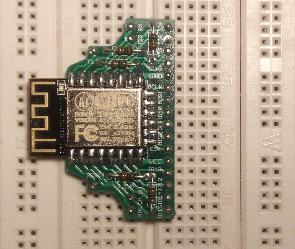
3.3. Plugging adapter
Adapter should be inserted to straddle the centerline of a breadboard like DIP ICs. That leaves tie points for all signals uncovered by the adapter itself. Following number of uncovered tie points is available:
| Signal | Uncovered tie points | Location according to the centerline | Pin type |
|---|---|---|---|
| RESET | 1 | left | Control |
| ADC | 4 | left | Analog |
| CH_PD | 3 | left | Control |
| GPIO16 | 4 | right | GPIO |
| GPIO14 | 4 | right | GPIO |
| GPIO12 | 4 | right | GPIO |
| GPIO13 | 4 | right | GPIO |
| VCC | 4 | right | Power |
| CS0 | 4 | right | SPI |
| MISO | 4 | right | SPI |
| GPIO9 | 4 | right | GPIO |
| GPIO10 | 4 | right | GPIO |
| MOSI | 4 | right | SPI |
| SCLK | 4 | right | SPI |
| GND | 4 | right | Power |
| GPIO15 | 4 | right | GPIO / Control |
| GPIO2 | 4 | right | GPIO / Control |
| GPIO0 | 4 | right | GPIO / Control |
| GPIO4 | 4 | right | GPIO |
| GPIO5 | 3 | left | GPIO |
| RX | 4 | left | Serial |
| TX | 1 | left | Serial |
Note
Due to space constrains all GPIO pins are labeled simply IO + number on a breakout board (i.e. GPIO10 is labeled IO10).